
Princeton Infrared Technologies Selected by United States Air Force to Develop Wafer Scale Hybridization for Building Large Area Devices
MONMOUTH JUNCTION, NJ – DECEMBER 13, 2023 – Princeton Infrared Technologies, Inc. (PIRT), global experts and innovators in indium gallium arsenide (InGaAs) imaging technology, announces it has been selected by the United States Air Force for a Phase II SBIR contract. This program will focus on the development of advanced concepts and an improved capability to hybridize heterogeneous, large format semiconductor materials, at the wafer level, for next-generation DoD Visible (VIS) and Infrared (IR) focal plane arrays (FPAs).
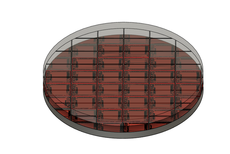
This program aims to develop wafer-scale hybridization of mixed material types (e.g. Si and III-Vs) for building large area imaging devices. This will be a significant improvement over the current costly methodology needed to produce large area FPAs using indium bump technology. PIRT will use wafer bond technology to attach an infrared detector wafer to a Si read out integrated circuit (ROIC) to form an FPA. PIRT will utilize a 1280x1024, 10µm pitch ROIC and hybridize 100mm detector wafers to assess the device’s yield across multiple 1280x1024 FPAs to determine projections for a larger 4k x 4k device.
Currently, most infrared FPAs are manufactured at chip scale. In this conventional approach, both the ROICs and detectors are processed as wafers, with indium bumps applied to each, followed by dicing them into individual chips. Subsequently, these individual chips are hybridized together to form an FPA. As the chip size increases (more pixels), additional pressure is required to compress the millions of indium bumps needed, making the process more intricate and challenging.
In wafer-scale hybridization, two wafers are bonded together using oxide to oxide bonds and metal contacts are connected using Cu pillars in the oxide. This is a departure from the current practice of producing infrared FPAs at the chip scale using indium bumps for the connections. With wafer-scale hybridization, the array size does not dictate the pressure needed to deform the current indium bumps to form very large format arrays. The same process can work for manufacturing hundreds of smaller arrays simultaneously. Moreover, this technique enables wafer-scale testing, which further drives down expenses. The process will initially start with 100mm detector wafers, but will transition to larger 200mm wafers at a later date.
Martin H. Ettenberg, Ph.D., President & CEO of Princeton Infrared Technologies, notes, “Winning this two-year program from the US Air Force to develop wafer scale hybridization for large devices represents a paradigm shift in cost-effective and efficient large area imager production. The technology is first being tested on InGaAs wafers. However, this process should be effective for all hybridized material types driving down cost of hybrid imagers, improving yields and allowing for very large formats without significant development costs.“