
What is InGaAs?
What is InGaAs?
Lattice matched InGaAs is deposited in very thin layers (several atomic layers) at a time on an InP substrate. It is called lattice matched because at 53% InAs and 47% GaAs (i.e. In.53Ga.47As) has the same atomic spacing as InP the substrate material that it is deposited on. This composition has an energy gap of 0.75eV which allows the detection of light up to 1.68 µm at 20C. Longer wavelengths of light can be captured with InGaAs alloys but more InAs is needed in the mixture. When this occurs one is no longer lattice matched. If the material is not lattice matched, meaning the atoms don’t line up anymore, then defects occur in the material. These defects produce significant noise, which makes it harder to detect the light. PIRT is working with our partners on new material structures to minimize the noise source, known in the industry as dark current (i.e. the noise produced when the material is biased in the dark). Lower dark current leads to more sensitive devices because there is less noise so one can detect smaller amounts of signal.
4” Substrates
Princeton Infrared Technologies is utilizing 4” InP substrates, which allow for more chips on wafer with greater uniformity. These are the largest substrates commercially available. This, in combination with an advanced III-V fabrication partner enables PIRT to produce InGaAs imagers at a higher quality and at a lower price than the competition. The state of the art fabrication facility “fab” has cassette to cassette processing, minimizing human touch with the wafers thus raising yield. In addition to the advance technology, our partner processes over 1,000 wafers per month of material enabling statistical process control to be deployed. Statistical process control enables the wafer processing to be consistent from run to run thus raising yield and quality. Most infrared fabs don’t run that many InGaAs wafers in a year, let alone a month, limiting their statistical process control and ability to have high yield which is one of the many reasons InGaAs detector arrays are so expensive. PIRT also has the advantage of not running its own fab so there is no large overhead expense passed on to the customer.
Advance Detector Structure
PIRT has a unique InGaAs detector structure, which allows for low noise and the ability to image from 0.4 to 1.7 µm with high Quantum Efficiency. Quantum Efficiency is how effective the material converts photons detected to electrons that can be measured. This detector structure has demonstrated very low dark currents that are competitive with others in the industry who have been manufacturing for years. This unique detector structure enables 100% fill factor in our detectors with no dead space. The detector has been manufactured to minimize the number of processing steps especially at elevated temperatures to maintain material quality.
All Digital Read Out Integrated Circuits
InGaAs detector arrays are a combination of detector material, which detects the light and turns the photons into electron-hole pairs. The number of electron-hole pairs is measured using a Read Out Integrated Circuit (ROIC). The ROIC typically made from Si CMOS makes a complete circuit with the detector material allowing the current from the detector to be converted to a voltage and stored. The combination of ROIC and detector material makes a focal plane array. There are two types of focal plane arrays (FPAs) - two-dimensional and one-dimensional. Two-dimensional are analogous to the imagers in your camera phone while one-dimensional arrays are analogous to the detectors in a fax machine, if something is scanned under them they can produce a two-dimensional picture. One-dimensional arrays are used in machine vision on production lines and in spectroscopy where each pixels detects a specific wavelength of light. The detector material transforms the light to current we can measure but the ROIC is the smarts behind the detector and allows for the various applications. Different ROICs enable different functionality.
Princeton Infrared Technologies deploys state of the art digital ROICs. These ROICs have 13- to 14-bit outputs and enable high speed and low noise circuits that enable fast frame rates with high sensitivity. PIRT utilizes ROICs that were designed with our specifications with outside design houses that specialize in advance CMOS ROIC design. PIRT's focus is to leverage many of the advances and benefits occurring in the visible imaging world into our infrared imaging engines. Princeton Infrared Technologies will also use commercial ROIC circuits to meet specific applications. We work with our customer to meet their application needs and that could take the form of designing a new circuit or purchasing an off the shelf circuit and integrating it with our detectors.
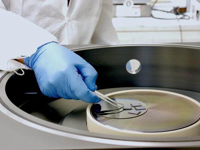
Advanced Hybridization
To form a focal plane array each detector has to be attached to its associated circuit on the ROIC. In a 1280x1024 array that is over 1.3 million connections! To be pleasing to the eye >99.5% of those connections need to be fully operable. In linear arrays the connection between the ROIC and InGaAs detector is generally done with wire bonds. This is where a very thin gold wire is attached to the detector and the ROIC. In two-dimensional arrays it is done with indium bumps. These are columns of indium that are placed on both the detector and ROIC. In this process each detector and ROIC chip are then carefully aligned in x, y, and z as well as tilt and individually pressed together with heat and pressure. Indium is used because many infrared materials are cooled and the indium allows for the thermal expansion differences of the two materials.
PIRT believes new more advanced 3D IC processes are needed to lower cost and improve yield in SWIR imagers. PIRT is working on 3D wafer-to-wafer hybridization of its detectors to ROICs. This has many advantages in terms of processing, we can post process all of the devices simultaneously to reduce cost and improve yield and uniformity. This technique will also lead to smaller pitch devices and lower cost for a given resolution.
Packaging and Electronics
Princeton Infrared Technologies, Inc. works with our customers to design and build the packaging and electronics needed to fit the application. PIRT is focused on low cost packages. We will look at using glass windows versus sapphire and ceramic and plastic packages versus the kovar and high end metal packages. PIRT sells the detectors with packages integrated with thermoelectric coolers (TECs) as well as bare die. We work with our customers to meet their needs and not upsell them to add value.
PIRT works with several electronic houses to provide support electronics to operate the arrays. IRcameras provides commercial imaging array electronics that work with our two-dimensional focal plane arrays. We sell the complete camera system as well as sell the focal plane array by itself.