
What is SWIR?
What is the SWIR wavelength region?
The shortwave infrared (SWIR) has various definitions, depending on the author. Like most definitions, the meaning of the label has also evolved over time. SWIR is a sub-region of the electromagnetic wavelength spectrum that scientists historically have called the Infrared and is included in the region that spectroscopists referred to as the Near Infrared (NIR). As detector technology developed, the NIR region was bounded by where the human eye can no longer see and where silicon detectors become transparent and lose sensitivity, which is slightly longer than 1 micron (1 µm) in wavelength. For the purposes of this website, which is provided by Princeton Infrared Technologies (PIRT) a SWIR imaging detector company, the SWIR region runs from 1000 to 2600 nm (1.0 to 2.6 µm). This is bounded on the shorter wavelength end by the NIR region from 750 to 1000 nm (0.75 to 1 µm) and on the longer side by the dominant atmospheric absorbance band from 2600 to 3000 nm (2.6 to 3.0 µm). This longer wavelength SWIR boundary is further re-enforced by the end of the transmission window for glass and quartz optics, which is around 2.6 µm.
As detector technology has developed, there are now low noise Vis-SWIR InGaAs imaging detectors that cover the visible to the middle of the SWIR range, 400 to 1700 nm (0.4 to 1.7 µm), such as the PIRT MVCam, and 1280SciCam. In the past, to extend beyond 1700 nm required changing the InGaAs crystal, this introduced excess dark current and image non-uniformities that made such imaging detectors unattractive to the market, causing some to commercialize low quantum-efficiency (QE) technologies such as colloidal quantum dots (CQD). This is now changing. PIRT has just introduced, a megapixel camera that responds from 400 to 2050 nm (0.4 to 2.05 µm) utilizing a completely different detector structure, one using InGaAs/GaAsSb type-II super lattice (T2SL) technology. This is yielding superior image quality with QE response of >30% at 1550 nm and >20% at 1900 nm (at 1.55 and 1.9 µm) with no imaging artifacts.
Why are the SWIR, NIR-SWIR and Vis-SWIR bands valuable?
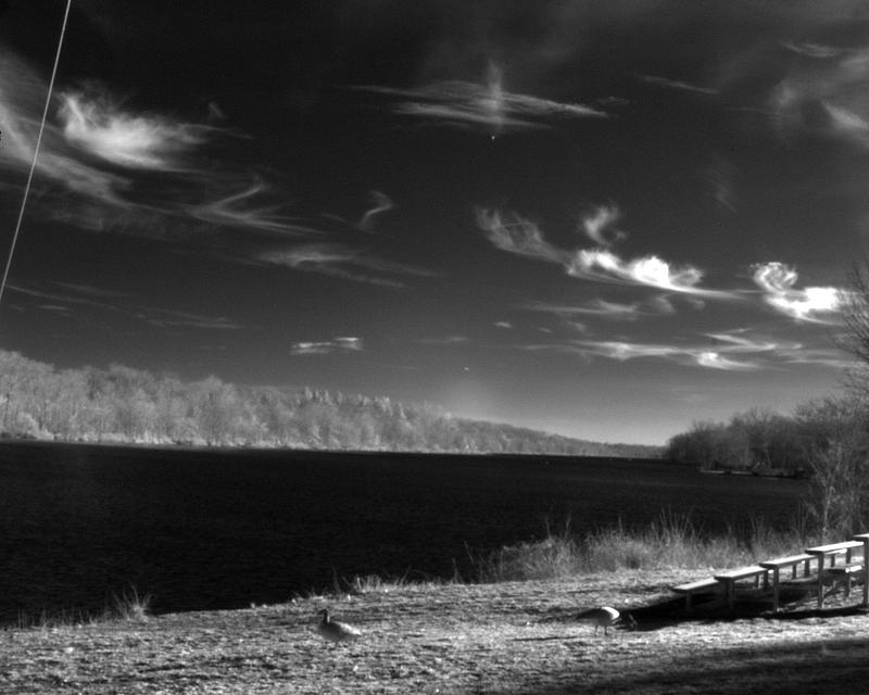
The SWIR wavelength range is important because, chemical signatures due to chemical absorption are imprinted on reflected or transmitted light. The images are easier for operators to understand because viewing NIR and SWIR images are like viewing visible light images. There is also reduced scattering in the SWIR band allowing for sharper images while looking through the atmosphere at objects far away. For special cases, the SWIR band has value for thermal imaging as well, such as when object temperatures are >100°C, or need to be viewed through glass or quartz optics or windows.
The principal advantages of the SWIR band are these imaging abilities:
- Sees farther in turbulent air than visible or NIR sensitive cameras,
- Sees with more clarity through obscurants than shorter wavelength cameras
- Sees through some opaque films:
- including seeing the under-drawings in artworks
- Sees the location of 'invisible' films
- 'Sees' chemical differences between materials, via reflectance or transmission, because of the materials' molecular vibrations:
- such as seeing differences between plastics for recycling
- or between pharmaceutical drug mixture proportions and grain sizes
- or between crops and foreign objects at food processing plants
- or between grains to sort by protein, fat, or moisture levels
- or sees the uniformity of moisture levels when processing foods, textiles, or paper
- or 'sees' presence of greenhouse gases like Methane (CH4)
- or to distinguish natural objects from camouflage or disguises
- in all the above, SWIR absorption imaging has advantages over MWIR absorption for remote (standoff) sensing of chemical properties
- Sees through silicon layers to inspect ICs circuit layer alignment or MEMS internal structures
- Sees the location of circuit faults in ICs by detecting their weak photoemissions
- Sees cracks in solar cells
- Sees defects in solar cells via imaging glow at the bandgap wavelengths from photoluminescence (light stimulated) or electroluminescence (bias stimulated)
- Sees the thermal emissions of hot objects of over 75°C, especially through windows or lenses
NIR-SWIR and Vis-SWIR cameras are valuable for:
- Hyper- and multi-spectral imaging when combining visible color characteristics with molecular chemical detection improves sorting operations such as:
- Recycled plastics
- Grooming foreign debris and packaging materials from agricultural materials
- Evaluating crop health by monitoring chlorophyll, nitrogen and moisture levels
- Detecting battlefield beacons, illuminators, range finders and target designators of all wavelengths, whether visible or covert
- Broad band imaging where only one optical path is practical due to available size, weight or power (SWaP):
- Note that for applications where visible wavelengths are scattered, switching into the path a long pass filter will help a Vis-SWIR detector reject the scattering wavelengths
How are the SWIR wavelengths imaged?
Imaging detectors have an absorbance layer that receives light photons and absorb their energies. To be a good detector they must be able to convert the energies into an electrical current, rather than into heat or even reflecting the photons away. In materials that do this conversion well the absorbance layer is typically a semiconductor crystal whose bandgap energy is less than the energy carried by the photon's wavelength.
For visible and NIR wavelengths, the Silicon (Si) molecule is a good detecting material. Depending on the detector structure Si can convert over 90% of photons into electrons, a measure known as Quantum Efficiency (QE). However, as the wavelengths lengthen past 900 nm (0.9 µm), the efficiency in capturing photons becomes weaker and photons start passing through Si so QE falls, and goes below 1 % past 1100 nm, even with processing tricks used to extend sensitivity.
For the NIR-SWIR range there are various materials that have been tried for imaging. Commercial production currently uses these molecules for detection: InGaAs, NIR extended Si, Ge, Si-Ge, PbSe colloidal quantum dots (CQD), InGaAs/GaAsSb Type 2 Superlattices, InSb, or HgCdTe. In general, for the 1000 to 1680 nm (1.0 to 1.68 µm) range, the material known as lattice matched InGaAs (which is really In.53Ga.47As) offer the best combination of high QE, dynamic range, and image quality with low Size, Weight and Power. When imaging applications need to cover 1000 to 2100 nm (1.0 to 2.1 µm), new solutions based on Type II superlattice structures that have layers of InGaAs alternating with GaAsSb are now available that provide the best QE and image quality of commercially available cameras. In the future one will see Type 2 Strained Layer Superlattices which are more complicated combinations of InGaAs/GaAsSb and these will allow detection to 2600nm. Several alternative products claim to reduce cost compared to InGaAs designs which manually hybridize the photodiode layer to the Read-Out Integrated Circuit (ROIC) for each Focal Plane Array (FPA). However, PIRT uses wafer-scale bonding to substantially reduce the assembly costs, while the so-called low-cost competitors have discovered they still need costly thin-film processing to achieve reliable, and consistent imaging performance.
Comparison of SWIR imaging detector types
| Absorber | Full name | range | QE or D* | cooling | Cost |
|---|---|---|---|---|---|
| InGaAs | Indium Gallium Arsenide | 0.4 to 1.7 µm | High | +20°C | $$$ |
| T2SL InGaAs/GaAsSb | Type2 superlattice of Indium Gallium Arsenide layered with gallium arsenide antimony | 0.4 to 2.05 µm | Moderate | -30°C | $$$ |
| Ge | Germanium | 0.8 to 1.8 µm | Low at RT | +25°C | NA |
| SiGe | Silicon-Germanium | 0.4 to 1.5 µm | High in visible, low in SWIR | +20°C | NA |
| IR Extended Si | Silicon with surface treatment | 0.4 to 1.1 µm | High in visible, none in SWIR | ambient | $ |
| PbSe CQD | Lead sulfide colloidal Quantum Dots | 0.4 to 2.1 | High in visible, low in SWIR | +20°C | $$ |
| InSb | Indium Antimonide | Tuned for 1 to 5 µm | Low | -150°C | $$$$$ |
| HgCdTe | Mercury Cadmium Telluride | Tuned for 1 to 5 µm | Low | -200°C | $$$$$ |
NA: not available in 2022